This is a standard step-up (Boost) DC-DC converter topology. It takes the +12V source voltage and increases it up to the 45V–90V range required to illuminate the TV’s LED strips.
I can help guide you through the next steps in fixing your board.
Technicians often consult the TP.V56.PB801 schematic diagram to resolve specific, recurring hardware failures. Symptom 1: Completely Dead Board (No Standby LED)
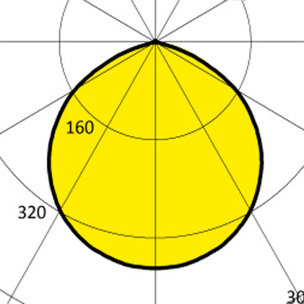
Measure DC voltage across main filter capacitor. It should read ~160V (on 110V lines) or ~320V (on 220V lines).
The SPI Flash memory chips are prone to data corruption over time due to heat or power surges.
Holds the TV firmware. Pins for VCC (3.3V), GND, MOSI, MISO, and CLK are critical test points.
If all physical voltage rails (12V, 5V, 3.3V, 1.2V) are stable, this symptom pointing directly to corrupted software.


This is a standard step-up (Boost) DC-DC converter topology. It takes the +12V source voltage and increases it up to the 45V–90V range required to illuminate the TV’s LED strips.
I can help guide you through the next steps in fixing your board. Tp.v56.pb801 Schematic Diagram Pdf
Technicians often consult the TP.V56.PB801 schematic diagram to resolve specific, recurring hardware failures. Symptom 1: Completely Dead Board (No Standby LED) This is a standard step-up (Boost) DC-DC converter topology
Measure DC voltage across main filter capacitor. It should read ~160V (on 110V lines) or ~320V (on 220V lines). Technicians often consult the TP
The SPI Flash memory chips are prone to data corruption over time due to heat or power surges.
Holds the TV firmware. Pins for VCC (3.3V), GND, MOSI, MISO, and CLK are critical test points.
If all physical voltage rails (12V, 5V, 3.3V, 1.2V) are stable, this symptom pointing directly to corrupted software.